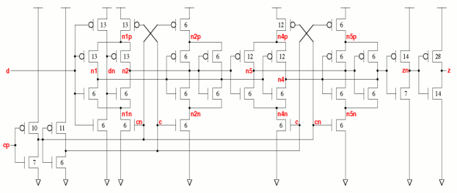
dfnt2 standard cell family

dfnt2v0x2
|
 |

|
dfnt2 standard cell family |
Rising clock edge D flip-flop |
|
||||||||||||||||||

|
D-type flip-flop with single x2 drive strength non-inverted output clocked on the rising edge of pin cp. Unusual design from an idea by Poojan Wagh at www.circuitdesign.info. The power numbers are given at the clock frequency both when the output is stable and when it changes. The setup and hold times are the maximum for pin d transition times up to 1500ps and for clock pin cp up to 670ps. The fanout 4 effort value is when the z output drives the cp input, as in a ripple counter. | |||||||||||||||||||
|
|
cell width | power | Generic 0.13um typical timing (ps & ps/fF), pin cp-z. | |||||||||||||||||
| leakage | dynamic | tR=PropR+RampR×Load(fF), tF=PropF+RampF×Load(fF) | ||||||||||||||||||
| vsclib013 | gates | lambda | 0.13um | nW | nW/MHz | PinCap | Prop | Ramp | Setup | Hold | ||||||||||
| dfnt2v0x2 | 8.3 | 200 | 11.00 | 2.04 | clock only | 13.9 | cp | 2.3f | Rise | 236 | 2.12 | 248 | 395 | |||||||
| state change | 56.5 | d | 4.6f | Fall | 249 | 1.66 | 324 | 353 | ||||||||||||
| ||||||||||||||||||||
| Web data book for the vsclib. Vdd=1.2V, T=27°C, nominal process, generic 0.13um technology. Copyright © 2005-2008 Graham Petley. 23 DEC 2008 | ||||||||||||||||||||