xor2 standard cell family

2-I/P exclusive OR gate
xor2 symbol
      pin a  pin b  pin a  pin b
      inverting non-inverting 
   xor2v0x1   84  78  97 102
   xor2v1x1  88  71 106  87
   xor2v2x1  78  70 107 100
   xor2v3x1  86  84 126 122
   xor2v4x1  79  71 152 121
   xor2v5x1  81  78 126 123
   xor2v6x1  92  81 120 126
   xor2v7x1 166 171 124 111
   xor2v8x1 155 122 127 102

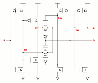
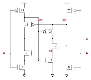
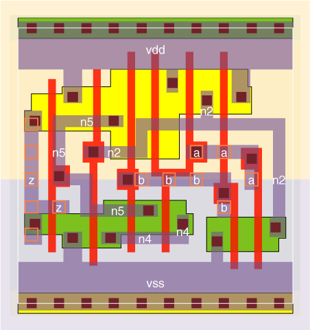
There are a number of ways to implement an XOR gate, and 9 of them are shown here.
- xor2v0 has the smallest number of transistors.
- xor2v1 is the classic two inverters with transfer gate onto the output node.
- xor2v2 is an alternative inverter plus transfer gate configuration.
- xor2v3 is an aoi22 with input inverters.
- xor2v4 is an oai22 with input inverters.
- xor2v5 is the aoi22 or oai22 with the connexion for the parallel P or N  transistors removed.
- xor2v6 is like the xor2v5 but with a connexion for both the parallel P or N  transistors.
- xor2v7 is a 2-NAND and OR-NAND combination with output buffering inverter. The schematic came from a public web site; the layout uses wsclib rules.
- xor2v8 is a xnr2v1 with an inverter output. This is a common style in commercial standard cell libraries.
XOR2 gates are one of the most common gate types: in most designs they are amongst the top-10 used cells. Their speed has a direct impact on overall circuit performance, as they are widely used in arithmetic functions. The 9 variants here have been characterised in the generic 0.13um technology, and a summary of their performance is shown in the table below. The fastest inverting gate is the xor2v2 on pin b. The fastest non-inverting gate is the xor2v1 on pin b, but this is slow for pin a. The xor2v0 is slower but smaller.
The xor2v3/v4/v5/v6 gates have very similar performances. The ones with larger diffusion parasitic capacitances have simpler layouts and lower metal parasitics. All these gates aren't really needed but are included to show their performance. The xor2v3x1 is similar to the sxlib xr2_x1.
The xor2v7 is fairly nasty. It's big and slow, and the transistors are wrongly sized. The non-inverting path is quicker because the inverting path uses 3 stage delays, rather than the single stage delay of the other gates. The xor2v8 is also a 2/3 stage delay gate which is slower than the others.
The average delay of each x1 gate and pin when driving just itself in a ring oscillator, inverting and non-inverting modes, is shown on the right.

z:(a^b) cell width power Generic 0.13um typical timing (ps & ps/fF), pin b.
leakage dynamic tR=PropR+RampR×Load(fF), tF=PropF+RampF×Load(fF)
wsclib013 gates lambda 0.13um nW nW/MHz PinCap PropR RampR PropF RampF
xor2v0x05 2.7  64 3.52  0.66  15.3  4.2f  72  5.49  57  3.89
xor2v1x05 3.0  72 3.96  0.62   9.6  4.2f  51  6.23  51  4.76
xor2v2x05 3.0  72 3.96  0.64  15.4  3.6f  71  4.68  63  2.97
xor2v8x05 3.0  72 3.96  0.83  19.2  4.3f  93  4.99 102  4.01
xor2v0x1 2.7  64 3.52  0.87  19.9  5.3f  72  4.16  57  2.96
xor2v1x1 3.0  72 3.96 1.14  16.2  7.1f  49  3.41  48  2.60
xor2v2x1 3.0  72 3.96 1.03  25.0  5.4f  73  2.64  62  1.93
xor2v3x1 3.0  72 3.96 1.29  19.3  6.2f  75  4.31  74  3.11
xor2v4x1 3.3  80 4.40 1.29  18.3  5.8f  70  4.29  74  3.06
xor2v5x1 3.0  72 3.96 1.29  18.7  6.1f  73  4.30  74  3.12
xor2v6x1 3.0  72 3.96 1.29  20.6  6.0f  80  4.31  76  3.10
xor2v7x1 3.3  80 4.40 1.18  26.4  5.9f 111  5.42 108  3.86
xor2v8x1 3.0  72 3.96  0.94  21.9  4.2f 100  3.33 111  2.68
xor2v0x2 4.7 112 6.16 1.82  40.1 10.3f  71  1.95  58  1.47
xor2v2x2 4.3 104 5.72 1.46  35.8  7.5f  72  1.85  63  1.38
xor2v8x2 3.0  72 3.96 1.11  26.5  4.2f 110  2.16 123  1.80
xor2v0x3 5.7 136 7.48 2.70  57.3 15.3f  69  1.34  54  0.94
xor2v0x4 6.7 160 8.80 3.59  75.2 20.5f  67  1.00  54  0.72
xor2v0x6 10.0 240 13.20 5.20 109.1 29.3f  68  0.70  54  0.49
xor2v0x05
 
Effort
FO4 Log.
a /\ 1.64 1.40
¯_ 1.96
b /\ 1.95 2.32
¯_ 2.13
xor2v0x05 schematic xor2v0x05 standard cell layout
xor2v1x05
 
Effort
FO4 Log.
a /\ 1.76 1.47
¯_ 2.15
b /\ 2.12 3.06
¯_ 1.98
xor2v1x05 schematic xor2v1x05 standard cell layout
xor2v2x05
 
Effort
FO4 Log.
a /\ 1.64 1.50
¯_ 1.92
b /\ 1.60 1.60
¯_ 1.90
xor2v2x05 schematic xor2v2x05 standard cell layout
xor2v8x05
 
Effort
FO4 Log.
a /\ 2.65 1.22
¯_ 2.35
b /\ 2.50 1.94
¯_ 2.50
xor2v8x05 schematic xor2v8x05 standard cell layout
xor2v0x1
 
Effort
FO4 Log.
a /\ 1.63 1.39
¯_ 1.97
b /\ 1.94 2.29
¯_ 2.08
xor2v0x1 schematic xor2v0x1 standard cell layout
xor2v1x1
 
Effort
FO4 Log.
a /\ 1.67 1.39
¯_ 2.01
b /\ 2.00 2.86
¯_ 1.86
xor2v1x1 schematic xor2v1x1 standard cell layout
xor2v2x1
 
Effort
FO4 Log.
a /\ 1.63 1.51
¯_ 1.85
b /\ 1.57 1.54
¯_ 1.80
xor2v2x1 schematic xor2v2x1 standard cell layout
xor2v3x1
 
Effort
FO4 Log.
a /\ 2.21 2.77
¯_ 2.67
b /\ 2.20 2.86
¯_ 2.56
xor2v3x1 schematic xor2v3x1 standard cell layout
xor2v4x1
 
Effort
FO4 Log.
a /\ 2.13 2.79
¯_ 2.88
b /\ 2.06 2.78
¯_ 2.47
xor2v4x1 schematic xor2v4x1 standard cell layout
xor2v5x1
 
Effort
FO4 Log.
a /\ 2.16 2.80
¯_ 2.67
b /\ 2.14 2.86
¯_ 2.57
xor2v5x1 schematic xor2v5x1 standard cell layout
xor2v6x1
 
Effort
FO4 Log.
a /\ 2.30 2.87
¯_ 2.63
b /\ 2.14 2.76
¯_ 2.63
xor2v6x1 schematic xor2v6x1 standard cell layout
xor2v7x1
 
Effort
FO4 Log.
a /\ 3.51 3.30
¯_ 2.98
b /\ 3.31 2.71
¯_ 2.97
xor2v7x1 schematic xor2v7x1 standard cell layout
xor2v8x1
 
Effort
FO4 Log.
a /\ 2.57 0.81
¯_ 2.27
b /\ 2.29 1.30
¯_ 2.20
xor2v8x1 schematic xor2v8x1 standard cell layout
xor2v0x2
 
Effort
FO4 Log.
a /\ 1.59 1.35
¯_ 1.95
b /\ 1.86 2.14
¯_ 2.00
xor2v0x2 schematic xor2v0x2 standard cell layout
xor2v2x2
 
Effort
FO4 Log.
a /\ 1.61 1.50
¯_ 1.84
b /\ 1.55 1.48
¯_ 1.78
xor2v2x2 schematic xor2v2x2 standard cell layout
xor2v8x2
 
Effort
FO4 Log.
a /\ 2.59 0.54
¯_ 2.29
b /\ 2.21 0.87
¯_ 2.09
xor2v8x2 schematic xor2v8x2 standard cell layout
xor2v0x3
 
Effort
FO4 Log.
a /\ 1.54 1.30
¯_ 1.86
b /\ 1.83 2.13
¯_ 1.96
xor2v0x3 schematic xor2v0x3 standard cell layout
xor2v0x4
 
Effort
FO4 Log.
a /\ 1.50 1.26
¯_ 1.85
b /\ 1.81 2.11
¯_ 1.97
xor2v0x4 schematic xor2v0x4 standard cell layout
xor2v0x6
 
Effort
FO4 Log.
a /\ 1.52 1.26
¯_ 1.85
b /\ 1.81 2.10
¯_ 1.95
xor2v0x6 schematic xor2v0x6 standard cell layout