Prior art from Logical Effort book
The book Logical Effort, Designing Fast CMOS Circuits by Sutherland, Sproull and Harris published in 1999 splits a gate's delay into two parts: a fixed delay p, called parasitic or Prop delay; and a load dependent delay f called the effort delay. These delays are made independent of the technology by finding the technology time constant τ. Then the delay d of a gate is given byd = τ ( p+f )
For a path with more than one gate, the most efficient implementation occurs when the effort delay f is the same for each gate. The critical path is the one where this value of f is the smallest. Actually this is only true when there is no branching. When there is branching the stage effort should obey the relationship
g1h1 =
b2g2h2 ;
g2h2 =
b3g3h3 ; …
gi-1hi-1 =
bigihi ; from which
g1h1 =
b2g2h2 =
b2b3g3h3 =
b2b3b4g4h4
The effect of this will be explored at a later date.
To find the critical path then,
- Take the path delay D (350ps) and divide by the constant τ (9.7ps) which gives a value of 36.2.
- List every path from each input to each output and sum its parasitic delays. The path parasitic delay is referred to as P and is independent of the load.
- Subtract this parasitic delay P from the path delay D to give the effort delay DF.
- Divide the effort delay DF by the number of stages N to get the stage effort f.
- The path with the smallest stage effort f is the critical path.
All the gates on the critical path then take this value of stage effort f. Other paths which also include these gates have their effort delay DF reduced by the value of f.
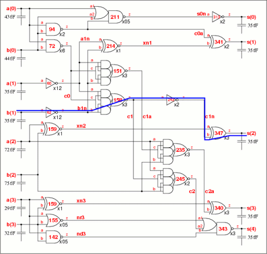
4-bit adder critical paths example
The table below shows the calculation for the critical paths. The path from a(1) to s(3) has the highest total parasitic delay P, the smallest effort f per stage and is the most critical. An effort f=3.1 is applied to all four instances along the path, which are highlighted.
| Path delay | P | DF | f | |||||
| a(1)- | -a1n- | -c1a- | -c2a- | -s3- | -s(3) | 24.0 | 36.2-24.0=12.2 | 12.2÷4=3.1 |
| b(1)- | -b1n- | -c1a- | -c2a- | -s3- | -s(3) | 23.7 | 36.2-23.7-3×3.1=3.4 | 3.4÷1=3.4 |
| b(1)- | -b1n- | -c1- | -c1n- | -s2- | -s(2) | 21.6 | 36.2-21.6-3.4=11.2 | 11.2÷3=3.7 |
| a(0)- | -c0- | -c1- | -c1n- | -s2- | -s(2) | 21.2 | 36.2-21.2-3×3.7=3.8 | 3.8÷1=3.8 |
| -c1a- | -c2a- | -s3- | -s(3) | 23.2 | 36.2-23.2-3×3.4=3.8 | |||
| a(0)- | -c0- | -c1- | -c2- | -s4- | -s(4) | 21.0 | 36.2-21.0-3.7-3.8=7.7 | 7.7÷2=3.8 |
| a(1)- | -a1n- | 21.7 | 36.2-21.7-3.7-3.1=7.7 | |||||
| b(1)- | -b1n- | 21.4 | 36.2-21.4-3.7-3.4=7.7 | |||||
| a(1)- | -a1n- | -xn1- | -s1- | -s(1) | 23.4 | 36.2-23.4-3.1=12.4 | 12.4÷2=6.2 | |
| … more critical paths … | ||||||||
| a(3)- | -nd3- | -s4- | -s(4) | 8.9 | 36.2-8.9-3.8=23.5 | 23.5÷1=23.5 | ||
These four instances now have their stage efforts fixed. The next path from b(1) to s(3) has only one instance, b1n whose stage effort is not fixed. The effort delay DF has the three known stage efforts subtracted to give a value of 3.4 which is applied to the instance b1n.
The third path from b(1) to s(2) is the next most critical. The stage effort of instance b1n is fixed and subtracted to give the effort delay DF of 11.2. This is divided equally over the three highlighted instances c1, c1n and s2 as a stage effort of 3.7.
The algorithm continues until the least critical path from a(3) to s(4) where a stage effort of 23.5 is applied to instance nd3. The stage efforts of all the cells is shown in the top schematic on the right Fig 8a. The critical path is the one with the lowest stage effort.
Converting stage efforts to delay
The stage effort is f = gh where g is the logical effort and h is the electrical effort. The logical effort comes from the library analysis (eg see Figure 5.11 in the Logical Effort book), and the electrical effort h = COUT /CIN is used to calculate the input pin capacitance of each gate.The cell with the next highest pin capacitance is chosen instead of the nearest cell. This leads to an overbuffered circuit, so to compensate the load capacitance is reduced by 20% to 28fF. This isn't very nice, as this kind of arbitrary allocation of margin can work for one circuit but not for another, and generally needs to be calibrated. But here we are just looking for a mapping that works as a demonstration of prior art, rather than the best mapping which is an exercise in its own right.
Take instance s4 as an example. The output load is 28fF and the input pin capacitances are calculated from the table below. The library cell with the next largest pin capacitances is then chosen, in this case an oai21v0x3. The CIN values are the ones adjusted for variations in logical effort between the cells as described in the section "Library analysis to derive the typical load value CS" on the Mapping to library cells using the patent algorithm page.
| Instance | Pin | f | g | COUT | CIN=gCOUT /f | oai21v0x2 | oai21v0x3 |
| s4 | a1 | 3.85 | 1.89 | 28.0 | 13.8 | 10.1 | 13.9 |
| a2 | 1.91 | 13.9 | 10.2 | 14.0 | |||
| b | 1.30 | 9.5 | 7.2 | 10.1 |
Working backwards from the outputs, each cell's load and ideal input capacitance can be found and used to select the right drive strength. The only exception, as before is to limit the gain or electrical effort h on non-inverting gates to 5.
The result is shown in the second schematic on the right, Fig 8b. There are four differences to the schematic produced by the patent algorithm (Fig 5c).
| Unbuffered adder results | |||||||
|---|---|---|---|---|---|---|---|
| Mapping algorithm | Fig | Instance | Critical path |
Gates | |||
| s4 | s3 | c1n | c0n | ||||
| area, 1 coeff CS | 5c | x4 | x4 | x3 | x1 | 351 | 75.7 |
| CIN, next up | 8b | x3 | x3 | x2 | x2 | 347 | 72.7 |
The prior art gives a better netlist. This might just be the result for this circuit, but in principle this should be the case because the cell selection is done directly using the input pin capacitance instead of indirectly through area estimates.
Buffered adder example
The stage efforts for the 4-bit adder with input buffers are shown in the third schematic on the right Fig 8c. These are used to derive input pin capacitances, then the nearest library cell and then the delay using the cell timing (Fig 8d). The differences between the three algorithms are shown in the table below.
| Buffered adder results | ||||||||
|---|---|---|---|---|---|---|---|---|
| Mapping algorithm | Fig | Instance | Critical path |
Gates | ||||
| xn2 | b2b | b1n | s0 | b0n | ||||
| area, 1 coeff CS | 7a | x2 | x8 | x12 | x1 | x1 | 371 | 86.7 |
| area, 2 coeffs CS0,CS0 | 7c | x3 | x12 | x8 | x1 | x2 | 354 | 89.3 |
| CIN, next up | 8d | x3 | x12 | x12 | x2 | x2 | 341 | 89.3 |
Similarities and differences to the patent algorithm
The theory of logical effort separates a path delay D into parasitic delay P and effort delay DF (see for example Table 1.4 from the Logical Effort book). The parasitic delay is a function of each gate type and is fixed. The effort delay is a function of the ratio COUT /CIN for each gate and is a minimum when the effort f=gh is the same for each gate. If the path has N stages, then f=DF /N and DF=D-P.The patent algorithm also allocates the effort equally to each logic stage, but without calculating the path parasitic delay P or effort delay DF. Instead an arbitrary effort of 3.6 is assigned to each logic stage and used to calculate each critical path. If a path is too slow or too fast, then the negative or positive slack is divided equally amongst the gates along the path so that each of them still bears an equal effort.
The patent directly links the cell area to its delay by deriving an area coefficient CS. This can allow delay constraints to be met while minimising area, albeit at the risk of a mismatch when selecting the library cell. There is a better match when two area coefficients CS0 and CS1 are used, but this is not considered in the patent. The prior art simply maps the calculated input capacitances for each cell to the nearest one in the library and hence if desired its area.
What is new in the patent then is
- The use of an arbitrary stage effort for initial timing and then adjusting it by compressing or stretching delays, rather than calculating each cell's stage effort by directly using the path parasitic delay.
- Linking area to delay by a single area coefficient so that area estimates can be made without using lookup tables to the library information.
- Using the area estimate of each cell instead of the input capacitance to select the cells from the library.