an3 standard cell family
3-I/P AND gate

There are two versions of these AND gates. The v0 cells have been designed for high speed, and the v4 cells for low power. For both versions, the output inverter P:N transistor ratio is 2 and the 3-NAND gate transistor ratio is 2.33 which sets the N and P transistors equal in size. The gain between the first and second stages is high for the v0 cells giving a gate optimised for speed. The gain in the v4 cells is set to 4, more suitable for a low power option.
z:(a*b*c)
cell width
power
Generic 0.13um typical timing (ps & ps/fF), pin c.
leakage
dynamic
tR=PropR+RampR×Load(fF), tF=PropF+RampF×Load(fF)
lambda
0.13um
nW
nW/MHz
PinCap
PropR
RampR
PropF
RampF
an3v4x1
50
2.75
0.59
15.3
2.0f
119
3.42
134
2.73
an3v0x1
50
2.75
0.91
18.2
3.6f
87
3.34
99
2.61
an3v4x2
50
2.75
0.90
21.9
2.6f
116
2.16
131
1.70
an3v0x2
50
2.75
1.27
24.7
4.5f
87
2.13
100
1.66
an3v0x4
80
4.40
2.24
39.8
7.1f
83
1.07
98
0.83

 an3v4x1

 an3v0x1
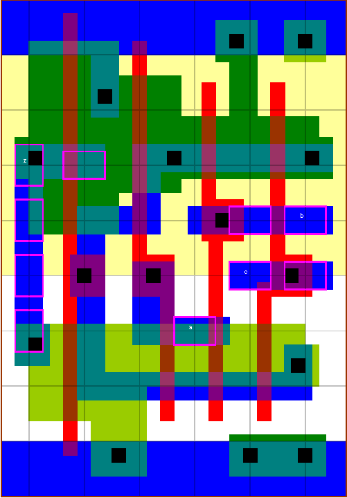
 an3v4x2
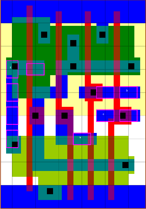
 an3v0x2

 an3v0x4