aoi21 standard cell family
2-AND into 2-NOR gate

3 cells with different drive strengths, each with a P/N ratio of about 2. The width of the N-transistor connected to pin b is designed to have a similar conductivity to the two series N-transistors in order to maintain a consistent output drive capability.
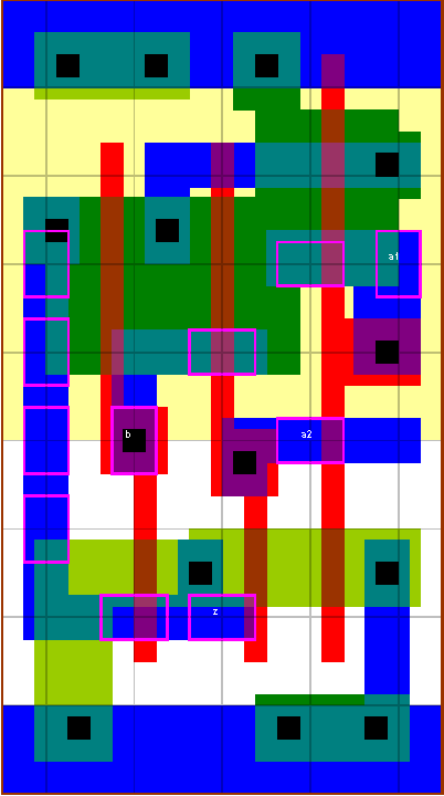
z:((a1*a2)+b)'
cell width
power
Generic 0.13um typical timing (ps & ps/fF), pin a2.
leakage
dynamic
tR=PropR+RampR×Load(fF), tF=PropF+RampF×Load(fF)
lambda
0.13um
nW
nW/MHz
PinCap
PropR
RampR
PropF
RampF
aoi21v0x05
40
2.20
0.34
5.0
3.1f
68
7.32
58
5.38
aoi21v0x1
40
2.20
0.53
7.6
4.9f
64
4.33
55
3.12
aoi21v0x2
70
3.85
1.09
14.8
9.6f
61
2.17
51
1.49
 aoi21v0x05

 aoi21v0x1

 aoi21v0x2