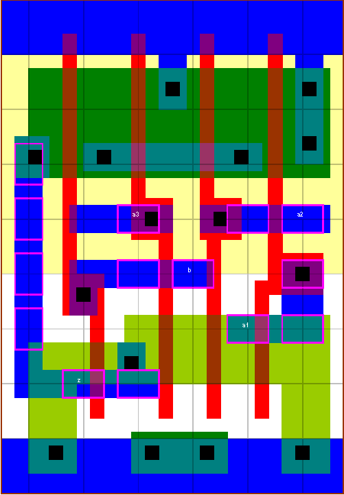
aoi31 standard cell family
3-AND into 2-NOR gate

3 cells with different drive strengths, each with a P/N ratio of about 2. The width of the N-transistor connected to pin b is designed to have a similar conductivity to the three series N-transistors so that the output drive is consistent from any input.
z:((a1*a2*a3)+b)'
cell width
power
Generic 0.13um typical timing (ps & ps/fF), pin a3.
leakage
dynamic
tR=PropR+RampR×Load(fF), tF=PropF+RampF×Load(fF)
lambda
0.13um
nW
nW/MHz
PinCap
PropR
RampR
PropF
RampF
aoi31v0x05
50
2.75
0.37
5.7
3.6f
73
7.37
57
5.25
aoi31v0x1
50
2.75
0.59
8.7
5.6f
69
4.35
57
3.25
 aoi31v0x05

 aoi31v0x1