bf1 & dly standard cell family
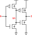
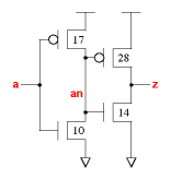
non-inverting buffers and delay cells

The buffers allow a large load to be driven with a small input capacitance. The delay cells have a large fixed delay and are mainly used for hold time fixing. The dly1 cell uses four chained inverters. The dly2 cells use two inverters with series transistors. The layout style maximises internal node parasitic capacitances, which contributes about 12ps to the dly1v0x05 fixed delay. The buffers have a P/N ratio of 2 (bf1v0), 1.5 (bf1v1) and 2.25 (bf1v2). The P/N ratio of 2 offers good output skew, while 1.5 is close to the fastest speed and 2.25 is balanced (if the mobility ratio = 2.25). The v0, v1, v2 & v5 versions have been designed for high speed, while the bf1v4x1 has been designed for minimum input capacitance.
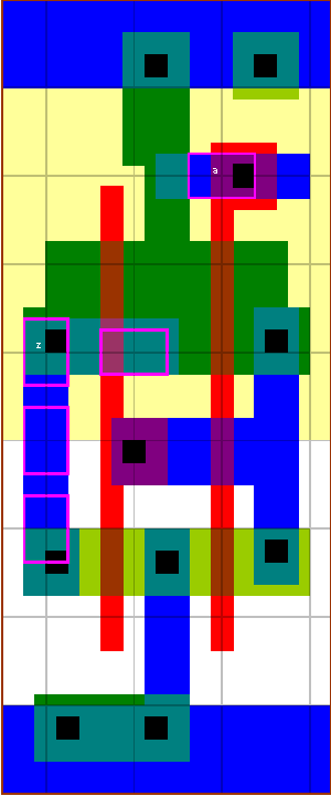
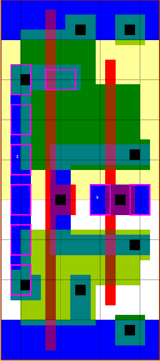
z:a
cell width
power
Generic 0.13um typical timing (ps & ps/fF)
leakage
dynamic
tR=PropR+RampR×Load(fF), tF=PropF+RampF×Load(fF)
lambda
0.13um
nW
nW/MHz
PinCap
PropR
RampR
PropF
RampF
dly1v0x05
60
3.30
0.69
25.1
2.2f
161
4.98
168
3.88
dly2v0x05
58
3.19
0.31
16.4
2.6f
171
8.76
219
6.90
dly2v0x1
58
3.19
0.54
24.7
2.4f
206
3.60
256
3.15
bf1v5x05
30
1.65
0.42
10.5
2.4f
61
4.97
73
3.86
bf1v4x1
30
1.65
0.45
12.4
1.7f
61
3.30
110
2.63
bf1v0x1
30
1.65
0.55
13.7
2.8f
62
3.30
75
2.56
bf1v5x1
32
1.76
0.62
15.4
3.8f
60
3.30
73
2.55
bf1v2x2
32
1.76
0.74
18.9
3.5f
68
2.20
82
1.91
bf1v0x2
32
1.76
0.79
19.9
3.6f
66
2.12
83
1.64
bf1v1x2
32
1.76
0.87
21.8
3.9f
63
2.12
83
1.22
bf1v5x2
32
1.76
0.97
22.9
5.5f
58
2.12
71
1.63
bf1v0x4
40
2.20
1.42
33.9
5.2f
70
1.06
86
0.82
bf1v5x4
50
2.75
1.94
38.3
10.3f
50
1.06
63
0.82
bf1v0x8
70
3.85
2.50
57.0
7.6f
72
0.57
88
0.44

 dly1v0x05

 dly2v0x05

 dly2v0x1
 bf1v5x05

 bf1v4x1

 bf1v0x1

 bf1v5x1

 bf1v2x2

 bf1v0x2
 bf1v1x2

 bf1v5x2

 bf1v0x4

 bf1v5x4
 bf1v0x8