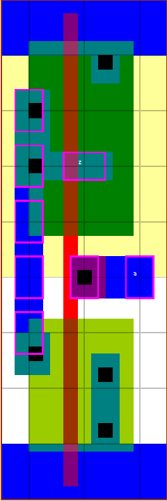
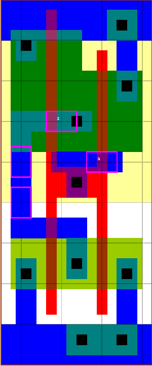
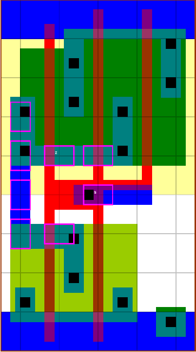
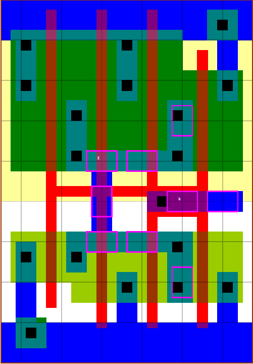
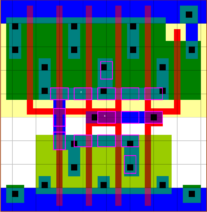
iv1 standard cell family
inverters

A set of inverters with P/N ratio of 2 (iv1v0), 1.5 (iv1v1) and 2.25 (iv1v2). The P/N ratio of 2 offers good output skew, while 1.5 is close to the fastest speed and 2.25 is close to balanced output skews.
z:a'
cell width
power
Generic 0.13um typical timing (ps & ps/fF)
leakage
dynamic
tR=PropR+RampR×Load(fF), tF=PropF+RampF×Load(fF)
lambda
0.13um
nW
nW/MHz
PinCap
PropR
RampR
PropF
RampF
iv1v0x05
20
1.10
0.21
3.3
2.3f
39
4.93
33
3.88
iv1v1x05
20
1.10
0.23
3.6
2.5f
40
4.92
29
3.00
iv1v0x1
24
1.32
0.31
4.8
3.4f
39
3.28
34
2.55
iv1v1x1
24
1.32
0.35
5.3
3.7f
40
3.28
31
1.95
iv1v2x2
24
1.32
0.45
6.7
4.8f
38
2.19
35
1.90
iv1v0x2
24
1.32
0.49
7.2
5.1f
38
2.11
34
1.63
iv1v1x2
24
1.32
0.54
8.0
5.7f
39
2.11
31
1.21
iv1v0x3
30
1.65
0.69
9.8
7.5f
37
1.48
33
1.14
iv1v0x4
30
1.65
0.97
13.3
10.2f
37
1.06
33
0.81
iv1v1x4
30
1.65
1.09
14.7
11.4f
38
1.05
30
0.61
iv1v0x6
40
2.20
1.39
18.9
14.4f
37
0.74
33
0.57
iv1v0x8
50
2.75
1.80
24.3
18.8f
36
0.57
33
0.44
iv1v0x12
70
3.85
2.77
37.4
29.1f
36
0.37
33
0.29

 iv1v0x05

 iv1v1x05
 iv1v0x1
 iv1v1x1
 iv1v2x2
 iv1v0x2
 iv1v1x2
 iv1v0x3
 iv1v0x4
 iv1v1x4
 iv1v0x6
 iv1v0x8
 iv1v0x12