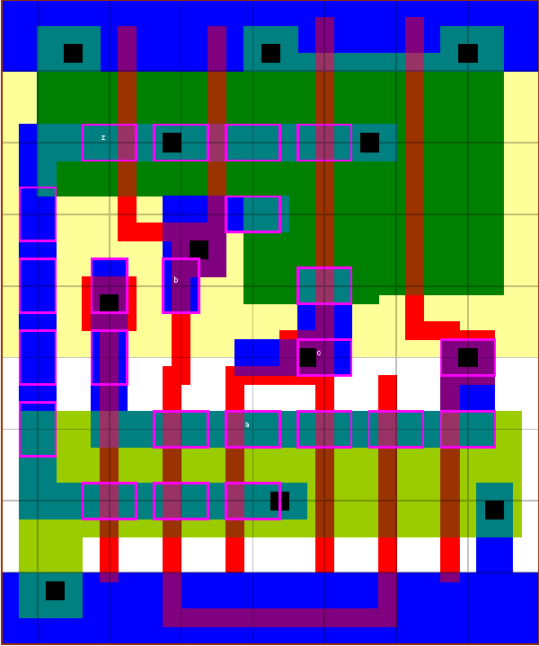
nd3 standard cell family
3-I/P NAND gate

The P/N ratio is set to 2.33, which is close to the P/N ratio of 2.29 which gives the fastest speed, as well as balanced rise and fall drive strengths. This means that the P:N transistors have the same size … r = KP·γ/KN = 1.
z:(a*b*c)'
cell width
power
Generic 0.13um typical timing (ps & ps/fF), pin c.
leakage
dynamic
tR=PropR+RampR×Load(fF), tF=PropF+RampF×Load(fF)
lambda
0.13um
nW
nW/MHz
PinCap
PropR
RampR
PropF
RampF
nd3v0x05
40
2.20
0.46
5.6
3.0f
54
5.96
43
5.10
nd3v0x1
40
2.20
0.92
9.8
5.4f
50
2.98
40
2.55
nd3v0x2
60
3.30
1.28
13.2
7.2f
48
2.12
38
1.82
nd3v0x3
70
3.85
1.85
18.5
10.2f
48
1.48
38
1.27
nd3v0x6
130
7.15
3.70
38.5
21.7f
49
0.74
39
0.64

 nd3v0x05

 nd3v0x1
 nd3v0x2

 nd3v0x3

 nd3v0x6