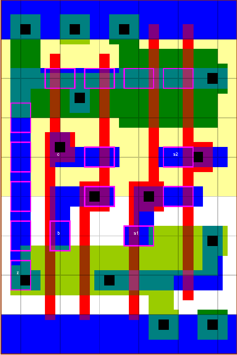
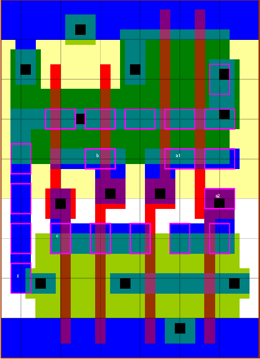
oai211 standard cell family
2-OR into 3-NAND gate

The P/N ratio is kept approx equal to 2. Series N-transistors are more conductive than series P-transistors, which explains the apparently larger P-transistors. The width of the P-transistors connected to pins b & c are designed to have a similar conductivity to the two series P-transistors, so that the output drive capability is consistent.
z:((a1+a2)*b*c)'
cell width
power
Generic 0.13um typical timing (ps & ps/fF), pin a2.
leakage
dynamic
tR=PropR+RampR×Load(fF), tF=PropF+RampF×Load(fF)
lambda
0.13um
nW
nW/MHz
PinCap
PropR
RampR
PropF
RampF
oai211v0x05
48
2.64
0.51
6.4
3.4f
86
7.35
57
5.15
oai211v0x1
52
2.86
0.86
10.4
5.7f
83
4.34
54
3.02
 oai211v0x05
 oai211v0x1