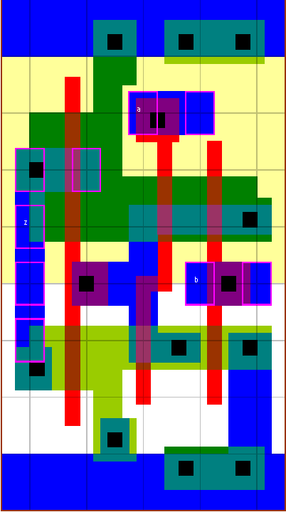
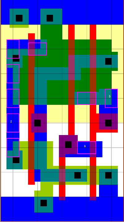
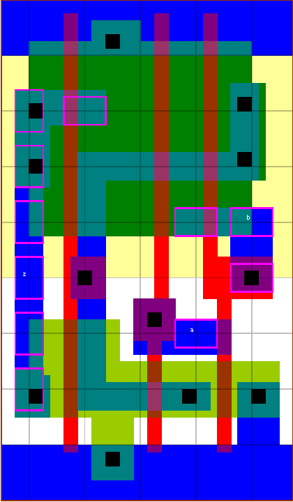
or2 standard cell family
2-I/P OR gate

The electrical gain between the NOR gate and output inverter is high in order to favour high speed in the v0 OR gates. The or2v4x1 has a smaller gain and is designed for a minimum input loading. The same function is performed by the nd2ab gates, which invert the inputs and drive the output thru a NAND gate. The nd2ab gates are faster than the or2 gates, but are bigger and consume more power.
z:(a+b)
cell width
power
Generic 0.13um typical timing (ps & ps/fF), pin b.
leakage
dynamic
tR=PropR+RampR×Load(fF), tF=PropF+RampF×Load(fF)
lambda
0.13um
nW
nW/MHz
PinCap
PropR
RampR
PropF
RampF
or2v4x1
40
2.20
0.55
13.3
2.3f
67
3.30
137
2.78
or2v0x1
40
2.20
0.69
16.0
3.6f
79
3.31
96
2.63
or2v0x2
42
2.31
0.99
22.7
4.7f
80
2.12
99
1.67
or2v0x4
64
3.52
1.73
35.5
6.8f
78
1.06
98
0.84
or2v0x8
102
5.61
2.98
62.9
10.7f
85
0.57
105
0.45
 or2v4x1
 or2v0x1
 or2v0x2
 or2v0x4
 or2v0x8


