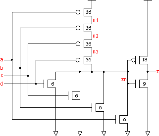
or4 standard cell family
4-I/P OR gate

The v0 cells have been designed for high speed. The or4v4x05 has been designed with a minimum input capacitance and has a high fall Prop delay because of the small P transistors on the Nor4 gate. The output inverter P:N transistor ratio is 2 and the 4-NOR gate transistor ratio is also 2 except where the 4-NOR gate N transistors must be set to a minimum width.
z:(a+b+c+d)
cell width
power
Generic 0.13um typical timing (ps & ps/fF), pin d.
leakage
dynamic
tR=PropR+RampR×Load(fF), tF=PropF+RampF×Load(fF)
lambda
0.13um
nW
nW/MHz
PinCap
PropR
RampR
PropF
RampF
or4v4x05
60
3.30
0.62
13.0
2.7f
74
4.98
177
5.15
or4v0x05
62
3.41
0.80
15.5
4.6f
87
4.99
120
4.63
or4v0x1
84
4.62
1.01
19.2
5.7f
94
3.31
114
2.90
or4v0x2
84
4.62
1.36
26.6
7.2f
101
2.13
116
1.79

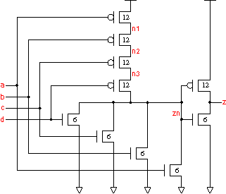 or4v4x05

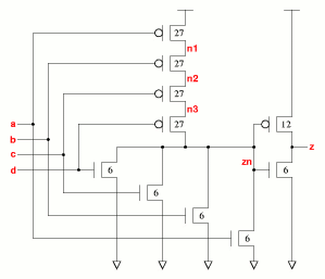 or4v0x05

 or4v0x1

 or4v0x2