| vlsitechnology.org /IR drop /1W core power | |
Example Calculation of Power Strap Width with 5LM, Same Resistivities and Widths, 1W Core Power |
IR Drop
- IR drop problem
- Power delivery
- chip illustration
- 1W core power
- 2W core power
- 15% power straps
- 1W 30% blocks
- 2W 30% RAM, 20% analog
- upper power straps
- reducing impact
- 1W power best
- 2W power best
- 1W best 30% blocks
- 2W best RAM, analog
- summary of method
- conclusions
- example 1
- example 2
Derivations
The power strap calculation follows 5 steps.
Step 1: Calculate Ipad and Vcore:
| Ipad = |
|
||
| = | 1⁄(1.2×16) = 0.052A |
| Vcore = |
|
||||||
| = | 1.14×(1−2×0.052×(0.025+0.025+0.1)⁄1.2 | ||||||
| = | 1.125V |
Step 2: Calculate the reference power supply conductance G:
| G = |
|
|||
| = | 7 ⁄ (4 × 0.07) = | 25 mhos |
Step 3 is to set out the values of kan, kwn, kcn and mn for each metal layer, and use these to calculate the value of L.
| ||||||||||||||||||||||||||||||||||||||||||||||||||||||
| kan and kcn are 100% because all power straps have the same space allocated and the metal resistivities are the same. kwn is 80% for all metal layers because the power strap widths and spacings are also all the same. | ||||||||||||||||||||||||||||||||||||||||||||||||||||||
Normally we can't calculate L directly because its value depends on p which we don't know. But in this case with m1‑5=0 we can
| L = | kw1kc1(1-ps)(1-m1(1-ka2p)(1-ka3p))+ |
| kw2kc2(1-m2(1-ka2p)(1-ka3p))+ | |
| kw3kc3(1-m3(1-ka2p)(1-ka3p))+ | |
| kw4kc4(1-m4(1-ka2p)(1-ka3p))+ | |
| kw5kc5(1-m5(1-ka2p)(1-ka3p)) | |
| = | ( 0.62 + 0.8 + 0.8 + 0.8 + 0.8 ) |
| = | 3.82 |
Step 4: Calculate the power strap allocation percentage p:
| p = |
|
||||||||
| = |
|
||||||||
| = | (0.701−0.222)×0.262 = 12.53% |
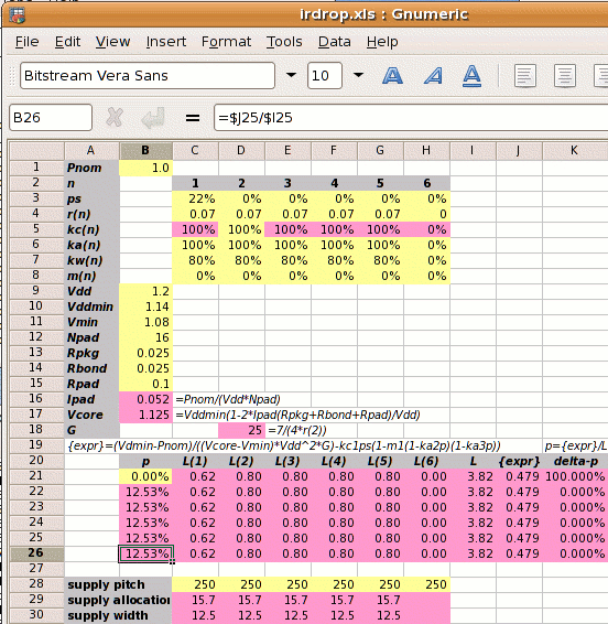
As shown on the right, a spreadsheet can be used to iterate to the answer. Yellow squares are user input; pink squares are calculated values.
Since in this example all the kan and kwn
are equal, the strap allocation and widths are the same for each layer.
If we decide to set the power strap pitch to 250µm,
then each Vdd and Vss supply strap width Wsn is:
| Wsn = | 250 × p × kw ⁄ 2 =250 × 0.1253 ×0.8 ⁄ 2 = 12.5µm |
Step 5: Calculate the new core size. If the initial core size estimate without power straps is x, then with power straps the core size becomes x′
| x′ = | x | = | x | = | x | = x+14.33% |
| √(((1-ka2p)(1-ka3p)) | √0.87472 | 0.8747 |
The value 14.33% is called the IR Drop Adder.
1W is not a very high power consumption, yet 12.5% of each metal layer must be allocated to extra power straps for the required power, and the die side increased by 14.3%.
| Design Attribute | Value | ||||
|---|---|---|---|---|---|
| Pnom | core power consumption | 1W | |||
| ps | fraction of metal-1 in the standard cells used for power supplies | 22% (for vsclib) | |||
| rn | resistivity of metal layer n in ohms per square | 0.07Ω per sq. | |||
| kan |
|
100% | |||
| kwn |
|
80% | |||
| mn | percentage of metal layer n blocked to power straps | 0% | |||
| Vdd | the nominal supply voltage | 1.2V | |||
| Vddmin | the minimum supply voltage, 5% less than nominal | 1.14V | |||
| Vmin | the desired voltage at the centre of the die, 10% less than the nominal | 1.08V | |||
| Npad | number of core Vdd or core Vss power pads | 16 | |||
| Rpkg | the resistance of the package leadframe | 25mΩ | |||
| Rbond | the resistance of the bond wire | 25mΩ | |||
| Rpad | the resistance of the bond pad | 100mΩ | |||
| kcn = |
|
This is a rather simplified example because the power strap widths and resistivities are the same for all the metal layers. Let's look at a more complex one.
