| vlsitechnology.org /IR drop /2W power, 30% RAM, 20% analog |
Example Calculation of Power Strap Width with 6LM, 30% RAM, 20% Analog, Different Resistivities and Widths, 2W Core Power |
IR Drop
- IR drop problem
- Power delivery
- chip illustration
- 1W core power
- 2W core power
- 15% power straps
- 1W 30% blocks
- 2W 30% RAM, 20% analog
- upper power straps
- reducing impact
- 1W power best
- 2W power best
- 1W best 30% blocks
- 2W best RAM, analog
- summary of method
- conclusions
- example 1
- example 2
Derivations
The horizontal power straps have half the allocation (or twice the pitch) of vertical ones; metal resistivities are different; core power consumption is 2W with 32 core Vdd and 32 core Vss pads; 30% core is RAM blocked to metal-4; 20% is analog blocked to all layers. It is the same as a previous example but with RAM and analog blocks.
Step 1: Calculate Ipad and Vcore:
| Ipad = |
|
||
| = | 2⁄(1.2×32) = 0.052A |
| Vcore = |
|
||||||
| = | 1.14×(1−2×0.052×(0.025+0.025+0.1)⁄1.2 | ||||||
| = | 1.125V |
Step 2: Calculate the reference power supply conductance G:
| G = |
|
|||
| = | 7 ⁄ (4 × 0.07) = | 25 mhos |
Step 3 is to set out the values of kan, kwn, kcn and mn for each metal layer, and use these to calculate the value of L.
| |||||||||||||||||||||||||||||||||||||||||||||||||||||||||||||||
| ¹78%=.07/.09; ²350%=.07/.02 | |||||||||||||||||||||||||||||||||||||||||||||||||||||||||||||||
The value of L depends on p which we don't know. We iterate to the solution and use p=0 for the first estimate.
| L = | kw1kc1(1-ps)(1-m1(1-ka2p)(1-ka3p))+ |
| kw2kc2(1-m2(1-ka2p)(1-ka3p))+ | |
| kw3kc3(1-m3(1-ka2p)(1-ka3p))+ | |
| kw4kc4(1-m4(1-ka2p)(1-ka3p))+ | |
| kw5kc5(1-m5(1-ka2p)(1-ka3p))+ | |
| kw6kc6(1-m6(1-ka2p)(1-ka3p)) | |
| = | ( 0.12 + 0.4 + 0.2 + 0.4 + 0.32 + 4.48 ) |
| = | 5.92 |
Step 4: Calculate the power strap allocation percentage p. The solution must be iterated, and the calculation below shows the first iteration.
| m1′ = | m1×(1-ka2p)(1-ka3p) |
| p = |
|
||||||||
| = |
|
||||||||
| = | (1.403−0.086)×0.169 = 22.23% |
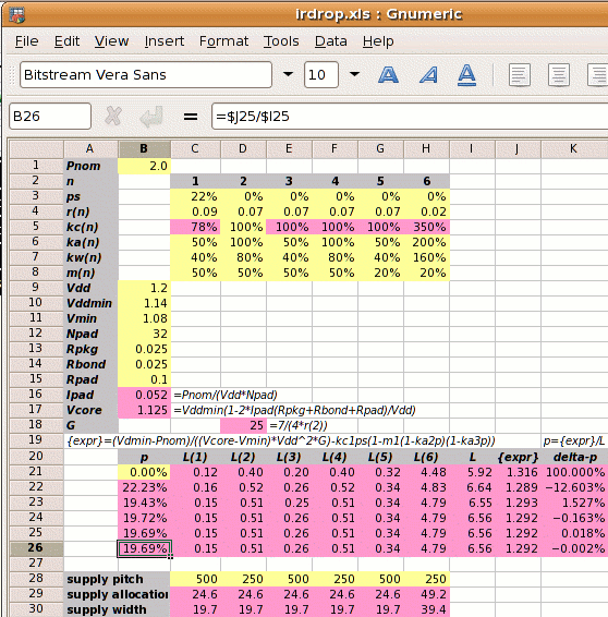
As shown on the right, a spreadsheet can be used to iterate to the answer of p=19.69%.
If the designer sets the power strap pitch, then the supply allocation for each metal layer n is pitch×kan×p⁄2 and the supply width is pitch×kwn×p⁄2. An example is shown in the spreadsheet on the right where we have chosen a vertical power strap pitch of 250µm.
Step 5: Calculate the new core size. If the initial core size estimate without power straps is x, then with power straps the core size becomes x′
| x′ = | x | = | x | = x+17.53% |
| √(((1−ka2p)(1−ka3p)) | √(0.8031×0.9015) |
The value 17.53% is called the IR Drop Adder.
The presence of the fixed blocks has increased the percentage of metal which must be allocated to power straps from 14.92% to 19.69%, an increase of 32%.
| Design Attribute | Value | ||||
|---|---|---|---|---|---|
| Pnom | core power consumption | 2W | |||
| ps | fraction of metal-1 in the standard cells used for power supplies | 22% (for vsclib) | |||
| r1 | resistivity of metal layer 1 in ohms per square | 0.09Ω per sq. | |||
| r2-5 | resistivity of metal layers 2-5 in ohms per square | 0.07Ω per sq. | |||
| r6 | resistivity of metal layer 6 in ohms per square | 0.02Ω per sq. | |||
| ka1,3,5 |
|
50% | |||
| ka4 |
|
100% | |||
| ka6 |
|
200% | |||
| m1-4 | metal layers 1-4 blocked to power straps | 50% | |||
| m5-6 | metal layers 5-6 blocked to power straps | 20% | |||
| Vdd | the nominal supply voltage | 1.2V | |||
| Vddmin | the minimum supply voltage, 5% less than nominal | 1.14V | |||
| Vmin | the desired voltage at the centre of the die, 10% less than the nominal | 1.08V | |||
| Npad | number of core Vdd or core Vss power pads | 32 | |||
| Rpkg | the resistance of the package leadframe | 25mΩ | |||
| Rbond | the resistance of the bond wire | 25mΩ | |||
| Rpad | the resistance of the bond pad | 100mΩ | |||
| kcn = |
|
