| vlsitechnology.org /IR drop /1W power with blocks improved |
Example Calculation of Power Strap Width with 30% Fixed Blocks, 1W Core Power |
IR Drop
- IR drop problem
- Power delivery
- 10% power straps
- standard cell
- chip illustration
- calculate width
- conductivity calc.
- strap width
- 1W core power
- 2W core power
- fixed blocks
- 1W 30% blocks
- 2W 30% RAM, 20% analog
- upper power straps
- die size impact
- examples' die size
- reducing impact
- 1W power best
- 2W power best
- 1W best 30% blocks
- 2W best RAM, analog
- summary of method
- conclusions
Derivations
Step 1: Calculate the voltage on the supply pad Vpad:
| Vpad = | Vddmin-2×Ipad×(Rlead+Rbond+Rpad) |
| = | 1.164 - 2 × 0.05 × (0.025 + 0.0125 + 0.05) |
| = | 1.155V |
Step 2: Calculate the reference power supply conductance G:
| G = | 7 |
| 4×r(2) | |
| = | 7 / (4 × 0.07) |
| = | 25 mhos |
Step 3: Set out the values of j(n), k(n) and m(n) for each metal layer, and use these to calculate the value of L.
| |||||||||||||||||||||||||||||||||||||||||||||||||
| ¹no M6 layer; | |||||||||||||||||||||||||||||||||||||||||||||||||
| L = | j(1)×k(1)×(1-ps)×(1-(1-p)×m(1)) + |
| j(2)×k(2)×(1-(1-p)×m(2)) + | |
| j(3)×k(3)×(1-(1-p)×m(3)) + | |
| j(4)×k(4)×(1-(1-p)×m(4)) + | |
| j(5)×k(5)×(1-(1-p)×m(5)) |
Since we don't know the value of p,
we estimate it. The answer then produced is used as the next
estimate unitl the value of p converges to a stable result.
Our first estimate for p will be 0%.
The table below performs Step 4, the calculation of the
power delivered by the standard cell power rails;
| P(S) = | (Vpad‑Vmin)×Vdd2×ps×(1‑(1‑p)×m(1))×j(1)×G |
| Vpad |
and Step 5, the calculation of the percentage of metal used by the power straps.
| p = | Vpad | × | Ptot-P(S) |
| (Vpad-Vmin)×Vdd2 | G×L |
| iter- ation |
estimated p px‑1 |
Step 3 L |
Step 4 P(S) |
Step 5 new p px |
delta p p (px‑px‑1)÷px |
|---|---|---|---|---|---|
| 1 | 0.00% | 4.044 | 0.365 | 6.70% | 100.000% |
| 2 | 6.70% | 4.161 | 0.375 | 6.40% | -4.595% |
| 3 | 6.40% | 4.155 | 0.375 | 6.42% | 0.196% |
| 4 | 6.42% | 4.156 | 0.375 | 6.42% | -0.008% |
| 5 | 6.42% | 4.156 | 0.375 | 6.42% | 0.000% |
Let us compare this solution p=6.42% with the previous one
p=14.87% assuming that our metal-1 to metal-4 Vdd and Vss
power straps are 5.5µm wide.
| Design Attribute | Value | |
|---|---|---|
| Ptot | core power consumption | 1W |
| ps | the fraction of metal-1 in the standard cells dedicated to power supplies | 22% (for vsclib) |
| r | the resistivity of the reference metal layer measured in ohms per square | 0.07Ω per sq. |
| Vdd | the nominal supply voltage | 1.2V |
| Vddmin | the minimum supply voltage, 3% less than the nominal | 1.164V |
| Vmin | the desired voltage at the centre of the die, typically 10% less than the nominal | 1.08V |
| Ipad | the current per supply pad | 50mA |
| Rlead | the resistance of the package leadframe | 25mΩ |
| Rbond | the resistance of a double bond wire | 12.5mΩ |
| Rpad | the resistance of two parallel supply pads | 50mΩ |

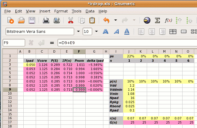
Using a spreadsheet to iterate to the solution.
| p | width m1-m4 |
width m5 |
pitch | core side mm |
|
|---|---|---|---|---|---|
| Previous power strap solution | 14.87% | 5.5µm | 5.5µm | 74µm | 9.397 |
| New power strap solution | 6.42% | 5.5µm | 11µm | 171µm | 8.548 |
The new solution has allowed the power strap pitch to go up from one every 74µm to one every 171µm. The core side is 849µm less and the core area is 17% less than the first solution, due to double bonding of supply pads, tighter Vddmin spec and wider metal-5 straps.