| vlsitechnology.org /IR drop /summary of method |
Summary of Supply Power Strap Width Calculation |
IR Drop
- IR drop problem
- Power delivery
- 10% power straps
- standard cell
- chip illustration
- calculate width
- conductivity calc.
- strap width
- 1W core power
- 2W core power
- fixed blocks
- 1W 30% blocks
- 2W 30% RAM, 20% analog
- upper power straps
- die size impact
- examples' die size
- reducing impact
- 1W power best
- 2W power best
- 1W best 30% blocks
- 2W best RAM, analog
- summary of method
- conclusions
Derivations
In order to calculate the width of power straps in a design, firstly the design attributes need to be set in a table like the one on the right.
Then the calculation proceeds in 5 steps.
Step 1: Calculate the voltage on the supply pad Vpad:
| Vpad = | Vddmin-2×Ipad×(Rlead+Rbond+Rpad) |
Step 2: Calculate the supply conductance G.
Normally this is the conductance of the metal‑2 layer.
| G = | 7 |
| 4×r(2) |
Step 3: Set out the values of
j(n), k(n) and m(n)
for each metal layer, and use these to calculate the value of L.
(L is the parallel metal conductivity coefficient.
That is, how much bigger the total metal conductivity
will be than the reference metal conductivity
due to multiple metal layers with different conductivities
and widths. j(n) says how much more conductive a
metal layer is than the value 1/r from the table at
the top right. k(n) sets out the relative widths
we want for each metal layer as a power supply.)
| metal layer | 1 | 2 | 3 | 4 | 5 | 6 | 7 | 8 |
|---|---|---|---|---|---|---|---|---|
| j(n) | ||||||||
| metal conductivity coefficient | ||||||||
| k(n) | ||||||||
| power strap coefficient | ||||||||
| m(n) | ||||||||
| core area blocked | ||||||||
The expression for L is:
| L = | j(1)×k(1)×(1-ps)×(1-(1-p)×m(1)) + |
| j(2)×k(2)×(1‑(1‑p)×m(2))+…+j(8)×k(8)×(1‑(1‑p)×m(8)) |
The value of L is a function of p, the amount of metal used for the power supplies and whose value we do not know. Since we don't know it, we estimate it. Our first estimate for p will be p=0%.
Step 3 uses the estimate for p to calculate L. Step 4 uses this value of L to calculate P(S), the power supplied by the standard cell supply lines.
| P(S) = | (Vpad‑Vmin)×Vdd2×ps×(1‑(1‑p)×m(1))×j(1)×G |
| Vpad |
Step 5 uses this value of P(S) to calculate a new value for p, since the rest of the power is supplied by the power straps.
| p = | Vpad | × | Ptot-P(S) |
| (Vpad-Vmin)×Vdd2 | G×L |
This new value of p is then used for the next calculation of L and the iteration continues until an acceptable level of accuracy has been reached.
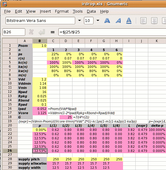
A spreadsheet can be set up to provide the answer as shown on the right. The yellow boxes are user input like core power consumption Ptot or the initial estimate for p. The pink boxes are calculated values.
The calculated value of p determines the power strap
width and pitch, and the new core size.
If we want to set the power straps to a width of w,
then their pitch is:
| horizontal pitch | M1 = | 2×w / (k(1)×p) |
| vertical pitch | M2 = | 2×w / (k(2)×p) |
| horizontal pitch | M3 = | 2×w / (k(3)×p) |
| vertical pitch | M4 = | 2×w / (k(4)×p) |
| horizontal pitch | M5 = | 2×w / (k(5)×p) |
| vertical pitch | M6 = | 2×w / (k(6)×p) |
If the core side before power strap insertion had a length
x, then afterwards it has a length
| x |
| √((1-k(2)×p)×(1-k(3)×p)) |
| Design Attribute | Value | |
|---|---|---|
| Ptot | core power consumption defined at nominal supply voltage | |
| ps | the fraction of metal-1 in the standard cells dedicated to power supplies | |
| r(1)‑r(n) | the metal layer resistivity in ohms per square | |
| m(1)‑m(n) | the percentage of each metal layer which is blocked to supply routing | |
| Vdd | the nominal supply voltage | |
| Vddmin | the minimum supply voltage from the device spec. | |
| Vmin | the desired voltage at the centre of the die, typically 10% less than the nominal | |
| Ipad | the current per supply pad | |
| Rlead | the resistance of the package leadframe | |
| Rbond | the resistance of the bond wire | |
| Rpad | the resistance of the core supply pad | |
j(n) is the ratio of the conductivity of metal layer n to the reference metal layer, normally metal‑2. For example, if metal-1 has a resistivity of 90Ω per sq. and metal-2 70Ω per sq., then j(1)=70/90=78%.
k(n) is the ratio of the width of the power strap in metal layer n to the width of the reference (metal-2) straps. If for example we do not want metal-1 power straps (except those already inside the standard cells), then k(1)=0%.
